The Manufacturing
Process
Printed circuit board processing and assembly are done in an incredibly smooth environment wherein the air and components can be saved free of contamination. Most digital manufacturers have their personal proprietary approaches, but the following steps might typically be used to make a two-sided published circuit board.
Making the substrate
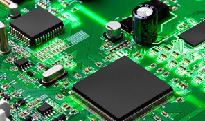
1 Woven glass fiber is unwound from a roll and fed thru a manner station The above illustrations display an enlarged phase of a PCB.
The above illustrations display an enlarged section of a PCB.
Wherein it is impregnated with epoxy resin either by way of dipping or spraying. The impregnated glass fiber then passes through rollers which roll the cloth to the favored thick-ness for the completed substrate and additionally get rid of any excess resin.
2 The substrate fabric passes through an oven wherein it’s far semicured. After the oven, the cloth is cut into big panels.
3 The panels are stacked in layers, alternating with layers of adhesive-sponsored copper foil. The stacks are placed in a press wherein they’re subjected to temperatures of approximately 340°F (a hundred and seventy°C) and pressures of 1500 psi for an hour or extra. This completely treatment plans the resin and tightly bonds the copper foil to the floor of the substrate fabric.
Drilling and plating the holes
4 Several panels of substrate, every huge sufficient to make several printed circuit forums, are stacked on top of each other and pinned together to keep them from shifting. The stacked panels are located in a CNC device, and the holes are drilled in line with the pattern determined when the boards were laid out. The holes are deburred to put off any excess material clinging to the rims of the holes.
5 The internal surfaces of the holes designed to offer a conductive circuit from one facet of the board to the alternative are plated with copper. Non-conducting holes are plugged to maintain them from being plated Printed Circuit Boardor are drilled after the character boards are cut from the larger panel.
Creating the published circuit sample at the substrate
The published circuit pattern can be created by means of an “additive” method or a “subtractive” technique. In the additive process, copper is plated, or added, onto the surface of the substrate inside the favored pattern, leaving the relaxation of the surface unplated. In the subtractive method, the complete floor of the substrate is first plated, and then the regions that aren’t a part of the favored pattern are etched away, or subtracted. We shall describe the additive system.
6 The foil surface of the substrate is degreased. The panels skip thru a vacuum chamber in which a layer of fantastic photoresist material is pressed firmly onto the complete floor of the foil. A tremendous photoresist cloth is a polymer that has the assets of turning into extra soluble whilst uncovered to ultraviolet mild. The vacuum ensures that no air bubbles are trapped between the foil and the photoresist. The published circuit pattern mask is laid on pinnacle of the photoresist and the panels are uncovered to an excessive ultraviolet light. Because the masks is clear within the regions of the published circuit sample, the photoresist in the ones areas is irradiated and will become very soluble.